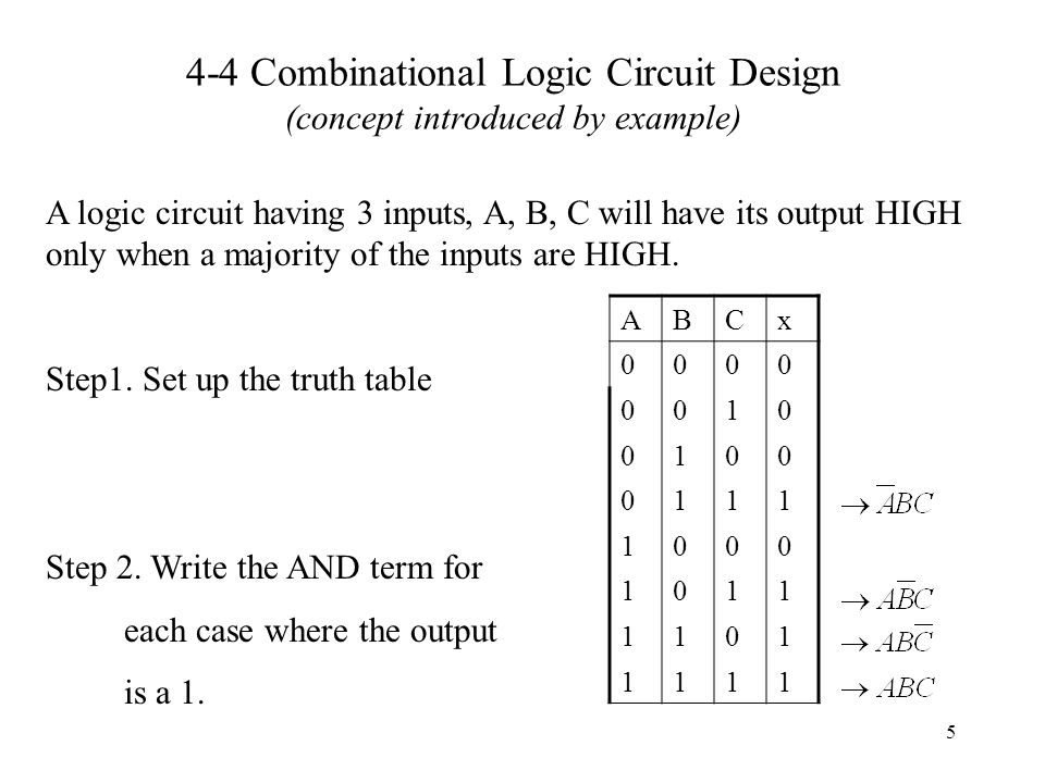
Design A Combinational Circuit That Generates Output As 1 Use K Map For Boolean Minimization
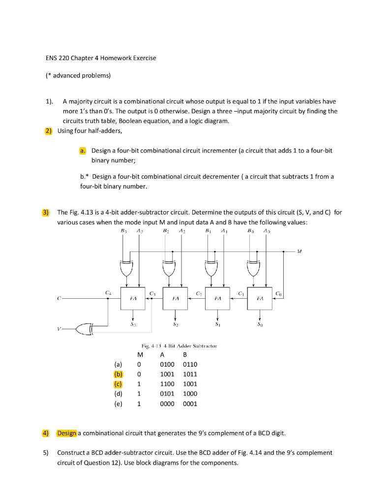
Solved Ens 220 Chapter 4 Homework Exercise Advanced Pro Chegg Com
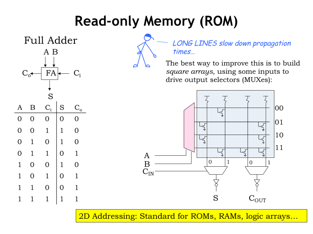
L04 Combinational Logic
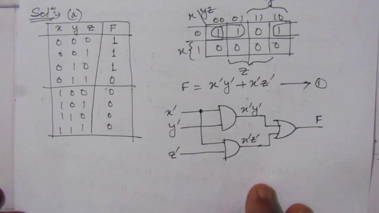
Q 4 4 Design A Combinational Circuit With Three Inputs And One Output A The Output Is 1 When Youtube
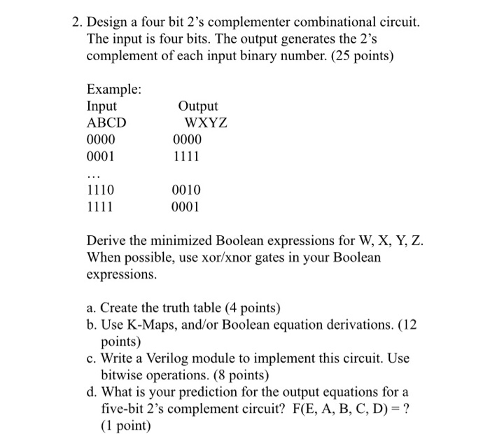
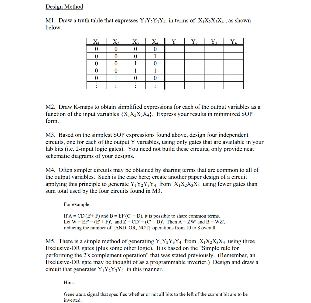
Solved 2 Design A Four Bit 2 S Complementer Combinationa Chegg Com
Solved Design A Combinational Circuit That Generates The 9 S C Chegg Com
Solved Design An Odd Parity Circuit This Is A Circuit That Ha Chegg Com

The truth table of the odd parity generator can be simplified by using k map as.
Design a combinational circuit that generates output as 1 use k map for boolean minimization. Example of combinational logic circuit. Draw the logic diagram using the and or gates and discuss its inference. The above boolean expression can be implemented by using one ex or gate and one ex nor gate in order to design a 3 bit odd parity generator. From the design specification obtain the truth table from the truth table derive the sum of products boolean expression.
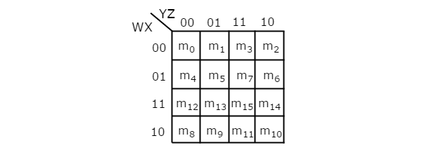
Minimization using k map the algebraic manipulation method is tedious and cumbersome. January 18 2012 ece 152a digital design principles 30 combinational design example 1 design specification design a logic network that takes as its input a 4 bit one s complement number and generates a 1 if that number is odd 0 is not odd label the inputs a b c and d where a is the most significant bit. Follow the above listed points to design the logic diagram as per the given statement. Example 2 consider the same expression from example 1 and minimize it using k map.
The logic diagram is drawn. Use karnaugh map to minimise the boolean. The previous state of input does not have any effect on the present state of the circuit. The output of combinational circuit at any instant of time depends only on the levels present at input terminals.
Understanding this process allows the designer to better use the cad tools and if need be to design critical logic. Next you will learn using guided worked examples how to design combinational logic circuits in minutes. P a b ex nor c. A combinational circuit can have an n number of inputs and m number of outputs.
The simplified boolean function for each output is obtained using k map tabulation method and boolean algebra rules. Repeated numbers should consider as single number design a combinational circuit that generates. Even though cad tools are used to create combinational logic circuits in practice it is important that a digital designer should learn how to generate a logic circuit from a specification. The output parity bit expression for this generator circuit is obtained as.
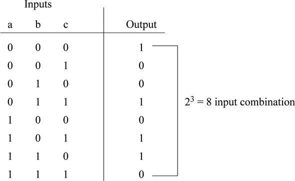
Design a combinational logic circuit with three input variables such that it will produce logic 1 output when one or two the input variables are logic 1 but not all the three. To convert a gate circuit to a boolean expression label each gate output with a boolean sub expression corresponding to the gates input signals until a final expression is reached at the last gate. Combinational logic circuit design. Combinational logic circuits design comprises the following steps.
The k map method is faster and can be used to solve boolean functions of upto 5 variables. As you can see the reduced circuit is much simpler than the original yet performs the same logical function. To design a combinational logic circuit use the following procedures.
Combinational Circuits Using Decoder Geeksforgeeks
Ch 4 Combinational Logic Circuits Ppt Download
Combinational Logic Logic Electronic Engineering Circuit
Digital Circuits K Map Method Tutorialspoint

1 Ee121 John Wakerly Lecture 4 Combinational Circuit Synthesis Abel Ppt Download
Solved Advanced Combinational Logic 2 S Complement Oper Chegg Com

Pin On Mrmgate
How Could I Design A Logic Circuit That Counts The Number Of 1s In 3 Inputs A B C And Outputs A Two Bit Binary Number Representing That Count Of 1s Quora
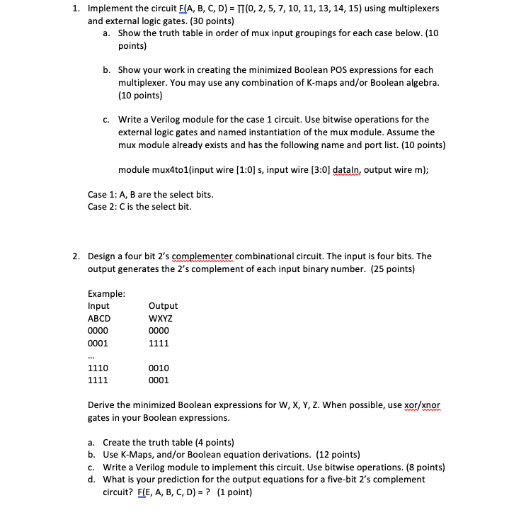
Solved 1 Implement The Circuit F A B C D 17 0 2 Chegg Com

Binary Logic And Gates Binary Logic Deals With Binary Variables I E Can Have Two Values 0 And 1 Binary Variables Can Undergo Three Basic Logical Ppt Download

Combinational Logic Circuits Using Logic Gates

Combinational Logic An Overview Sciencedirect Topics

Priority Encoder And Digital Encoder Tutorial

